
High density interconnect PCB (HDI) boards are generally manufactured by ceramic substrate method, and the more frequency of ceramic substrates, the higher the technical level of parts. Most of the general HDI boards are 1 time pressing, advanced HDI uses 2 or more ceramic substrate technology, and at the same time uses excellent PCB technology such as stacking holes, electroplating process filling holes, and laser immediately opening holes. When the relative density of the PCB increases beyond the 8layer board, the cost of manufacturing by HDI will be lower than that of the traditional complex pressing manufacturing. The mechanical strength and signal accuracy of HDI boards are higher than that of traditional PCBs. In addition, the HDI board has better improvements for microwave RF influence, radio wave influence, electrostatic induction release, heat conduction and so on. HD

In recent times, there has been a growing trend towards miniaturization and increased intelligence in electronic products. This has resulted in designers utilizing smaller PCB boards to accommodate these design requirements, made possible through the use of HDI High Density Interconnect PCB technology. HDI PCBs employ techniques such as blind vias, buried vias, micro vias, vias in pads, and very thin traces to accommodate more components in a smaller footprint while maintaining quality and performance.
In the manufacturing process of modern high-density electronic devices, HDI (High Density Interconnect) circuit boards play an important role. Among them, blind via is a key process in HDI circuit board manufacturing, which uses laser drilling technology to achieve more circuit connections in a limited space. SeekPCB will deeply study the importance of blind via in HDI board, and discuss the blind via manufacturing technology and the influence of blind via aspect ratio.

HDI (High Density Interconnect) circuit board is an indispensable part of modern electronic equipment, its high density circuit and complex functions make it an important solution to meet the needs of modern technology. In the manufacturing process of HDI PCB board, the buried via technology as a key process can realize more circuit connection. We will explore the importance of HDI board buried via technology, HDI PCB supplier selection, and the advantages of HDI high density interconnection.

With the rapid development of electronic technology, especially under the trend of smaller and miniaturized electronic products, HDI circuit boards came into being. It is a multilayer circuit board with complex internal layout, usually need to use high-density interconnection technology to achieve. So, what is the HDI pcb manufacturing process? The following will explain in detail for you.
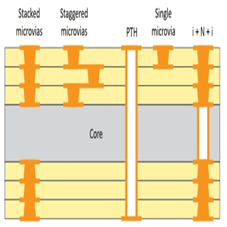
With the continuous development of electronic devices and increasing functions, the demand for PCB (printed circuit board) is also increasing. As a relatively new technology, HDI (high density interconnection) circuit board can meet the requirements of high speed, high performance and miniaturization. Among them, the micro via is an important part of the HDI circuit board, which plays a crucial role in the realization of high density interconnection.

What is the RF PCB?

What is a rigid-flex?

What is the difference between IC substrate and PCB?

What is a metal core PCB?

How do I know if my PCB is multilayer?

Why is copper used in printed circuit boards?
-
 2023-12-25High density interconnect PCB (HDI) boards are generally manufactured by ceramic substrate method, and the more frequency of ceramic substrates, the higher the technical level of parts. Most of the general HDI boards are 1 time pressing, advanced HDI uses 2 or more ceramic substrate technology, and at the same time uses excellent PCB technology such as stacking holes, electroplating process filling holes, and laser immediately opening holes. When the relative density of the PCB increases beyond the 8layer board, the cost of manufacturing by HDI will be lower than that of the traditional complex pressing manufacturing. The mechanical strength and signal accuracy of HDI boards are higher than that of traditional PCBs. In addition, the HDI board has better improvements for microwave RF influence, radio wave influence, electrostatic induction release, heat conduction and so on. HDRead More
 -
 2023-12-25In recent times, there has been a growing trend towards miniaturization and increased intelligence in electronic products. This has resulted in designers utilizing smaller PCB boards to accommodate these design requirements, made possible through the use of HDI High Density Interconnect PCB technology. HDI PCBs employ techniques such as blind vias, buried vias, micro vias, vias in pads, and very thin traces to accommodate more components in a smaller footprint while maintaining quality and performance.Read More
 -
 2023-12-07HDI (High Density Interconnect) circuit board is an indispensable part of modern electronic equipment, its high density circuit and complex functions make it an important solution to meet the needs of modern technology. In the manufacturing process of HDI PCB board, the buried via technology as a key process can realize more circuit connection. We will explore the importance of HDI board buried via technology, HDI PCB supplier selection, and the advantages of HDI high density interconnection.Read More
 -
 2023-12-07In the manufacturing process of modern high-density electronic devices, HDI (High Density Interconnect) circuit boards play an important role. Among them, blind via is a key process in HDI circuit board manufacturing, which uses laser drilling technology to achieve more circuit connections in a limited space. SeekPCB will deeply study the importance of blind via in HDI board, and discuss the blind via manufacturing technology and the influence of blind via aspect ratio.Read More


