
In recent times, there has been a growing trend towards miniaturization and increased intelligence in electronic products. This has resulted in designers utilizing smaller PCB boards to accommodate these design requirements, made possible through the use of HDI High Density Interconnect PCB technology. HDI PCBs employ techniques such as blind vias, buried vias, micro vias, vias in pads, and very thin traces to accommodate more components in a smaller footprint while maintaining quality and performance.
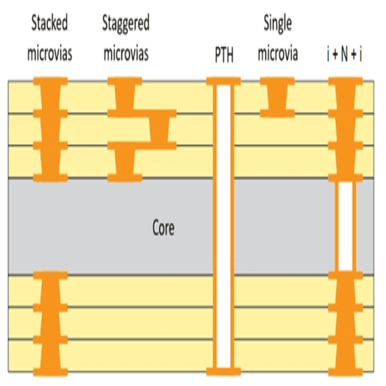
HDI (High Density Interconnect) circuit board is an indispensable part of modern electronic equipment, its high density circuit and complex functions make it an important solution to meet the needs of modern technology. In the manufacturing process of HDI PCB board, the buried via technology as a key process can realize more circuit connection. We will explore the importance of HDI board buried via technology, HDI PCB supplier selection, and the advantages of HDI high density interconnection.


-
 2023-12-25In recent times, there has been a growing trend towards miniaturization and increased intelligence in electronic products. This has resulted in designers utilizing smaller PCB boards to accommodate these design requirements, made possible through the use of HDI High Density Interconnect PCB technology. HDI PCBs employ techniques such as blind vias, buried vias, micro vias, vias in pads, and very thin traces to accommodate more components in a smaller footprint while maintaining quality and performance.Read More
 -
 2023-12-07HDI (High Density Interconnect) circuit board is an indispensable part of modern electronic equipment, its high density circuit and complex functions make it an important solution to meet the needs of modern technology. In the manufacturing process of HDI PCB board, the buried via technology as a key process can realize more circuit connection. We will explore the importance of HDI board buried via technology, HDI PCB supplier selection, and the advantages of HDI high density interconnection.Read More
 -


